Parent 

IBM 5150 to 5160 Comparison - 8255 PPI - I/O Pin Assignment


The 8255 is a chip on the IBM 5150 and IBM 5160 motherboard.
It has 24 general purpose I/O pins, segmented as 3 ports of 8 pins (ports A, B and C).

In the move from the 5150 to the 5160, IBM reassigned a lot of the 8255's general purpose I/O pins.  That was primarily because:
• The 5150's cassette port was removed
• The 5150's switch block SW2 was removed

Below, KSR means the Keyboard Shift Register chip (a 74LS322).


    = POST configures pin as an input
    = POST configures pin as an output
    = POST initially configures pin as an output, but near the end of the POST, reconfigures pin as an input

 
IBM 5150
 

IBM 5160
 
     
PA0 - PA7 Pin PB7 controls whether this byte is either:
1.  Switches in SW1; or
      2.  Received keyboard byte
Received keyboard byte  (see note 2)
     
PB0 Gate for timer (8253) chan 2  (diagram) [same as in 5150]
PB1 Data for speaker  (diagram) [same as in 5150]
PB2
HIGH:  Present switches 1 to 4 in SW2 to pins PC0 through PC3
LOW:  Present switch 5 in SW2 to pin PC0
Jumper E5  (see notes 3 and 5)
PB3
HIGH:  Cassette motor off  (diagram)
LOW:  Cassette motor on
HIGH:  Present switches 5 to 8 in SW1 to pins PC0 through PC3
LOW:  Present switches 1 to 4 in SW1 to pins PC0 through PC3
PB4 LOW: Enable detection of RAM parity errors on motherboard       (diagram) [same as in 5150]
PB5 LOW: Enable detection of RAM parity errors on expansion cards  (diagram) [same as in 5150]
PB6
HIGH:  Normal state of PB6
LOW:  Pull keyboard clock line to LOW  (see note 4)
[same as in 5150]
PB7
HIGH:  Clear KSR  +  Clear IRQ1  +  Present SW1 settings to port A
LOW:  Normal state of PB7
HIGH:  Clear KSR  +  Clear IRQ1
LOW:  Normal state of PB7
     
PC0 - PC3 Pin PB2 controls whether these 4 pins are either:
1.  Switches 1 to 4 in SW2; or     
2.  Switch 5 in SW2  (see note 1)
Pin PB3 controls whether these 4 pins are either:
      1.  Switches 5 to 8 in SW1; or
2.  Switches 1 to 4 in SW1
PC4 Cassette data in  (diagram) Monitor of speaker  (diagram)
PC5 Monitor of timer (8253) chan 2  (diagram) [same as in 5150]
PC6 RAM parity error occured on an expansion card  (diagram) [same as in 5150]
PC7 RAM parity error occured on motherboard  (diagram) [same as in 5150]


Note 1 When PB2 is low, PC0 corresponds to switch 5 within switch block SW2.
Because of the way the circuitry is wired, when PB2 is low, pins PC1, PC2 and PC3, will always read high.
   
Note 2 The '8255A I/O Bit Map' table in the 5160 Technical Reference includes "Diagnostic outputs" against port A.
That will be a reference to 'checkpoints' that the 5160's POST sends to port A.
More information on that is in note 15 at the bottom of here.
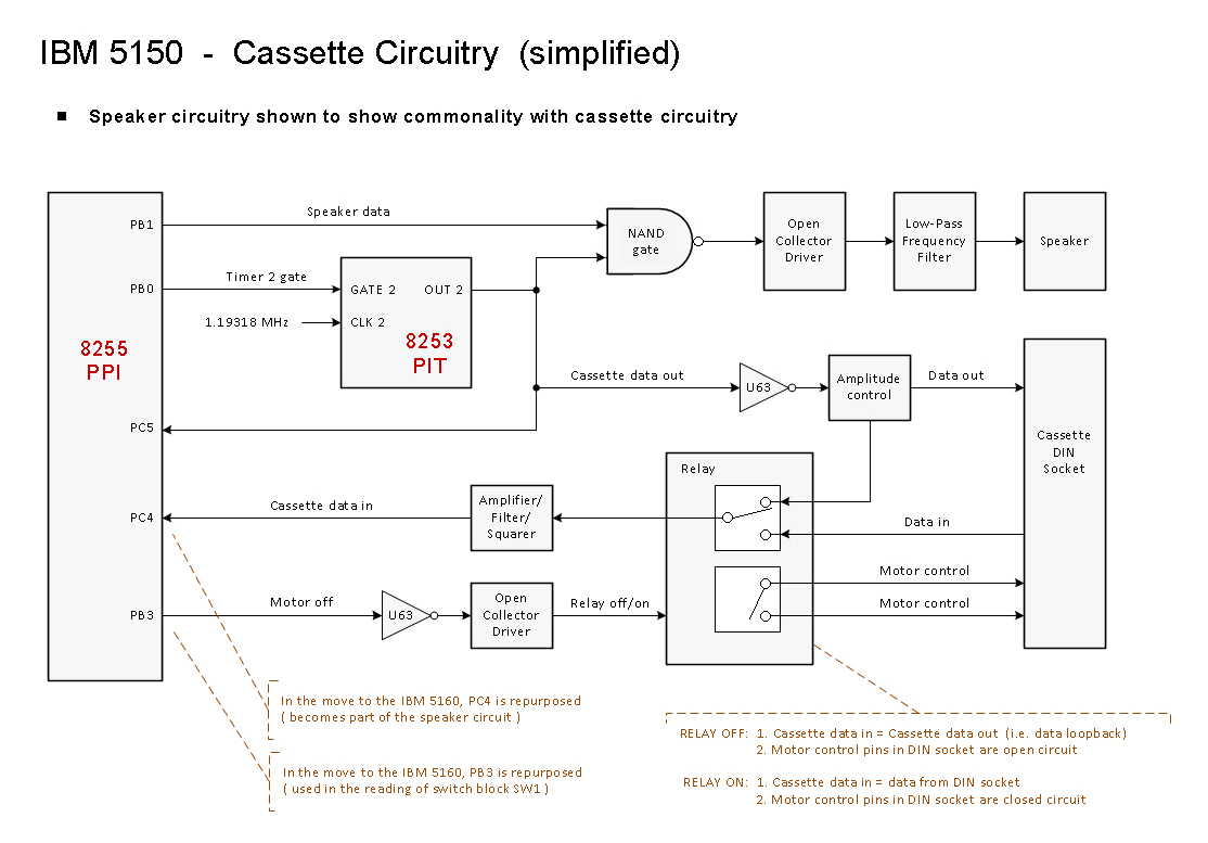
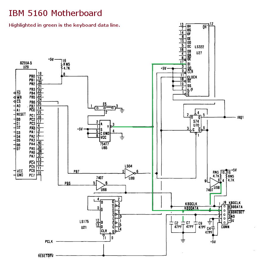
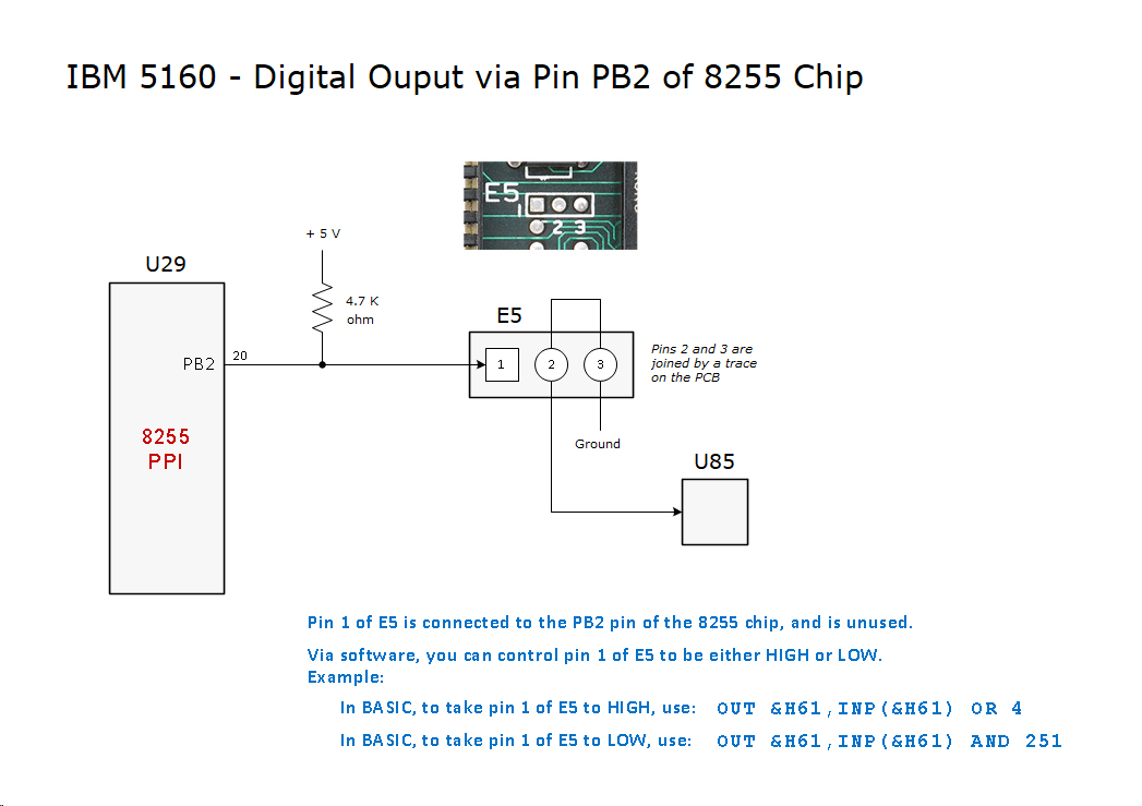
   
Note 3 The '8255A I/O Bit Map' table in the 5160 Technical Reference lists the usage of PB2 as 'Spare'.
The motherboard circuit diagram shows PB2 connected to jumper pad E5.
Per here, jumper pad E5 is part of the keyboard circuitry.
Pins 2 and 3 of E5 are normally connected, as seen by the wide PCB trace in the photos at here.
Should someone (?) decide to cut that trace, followed by connecting pins 1 and 2 together, then pin PB2 of the 8255 chip will control (via chip U85) the data line of the keyboard connector.
At one time, IBM must have seen reason to allow that.
But, with jumper pad E5 wired as default, pin PB2 of the 8255 is unused ('spare'), free for custom use - see here.
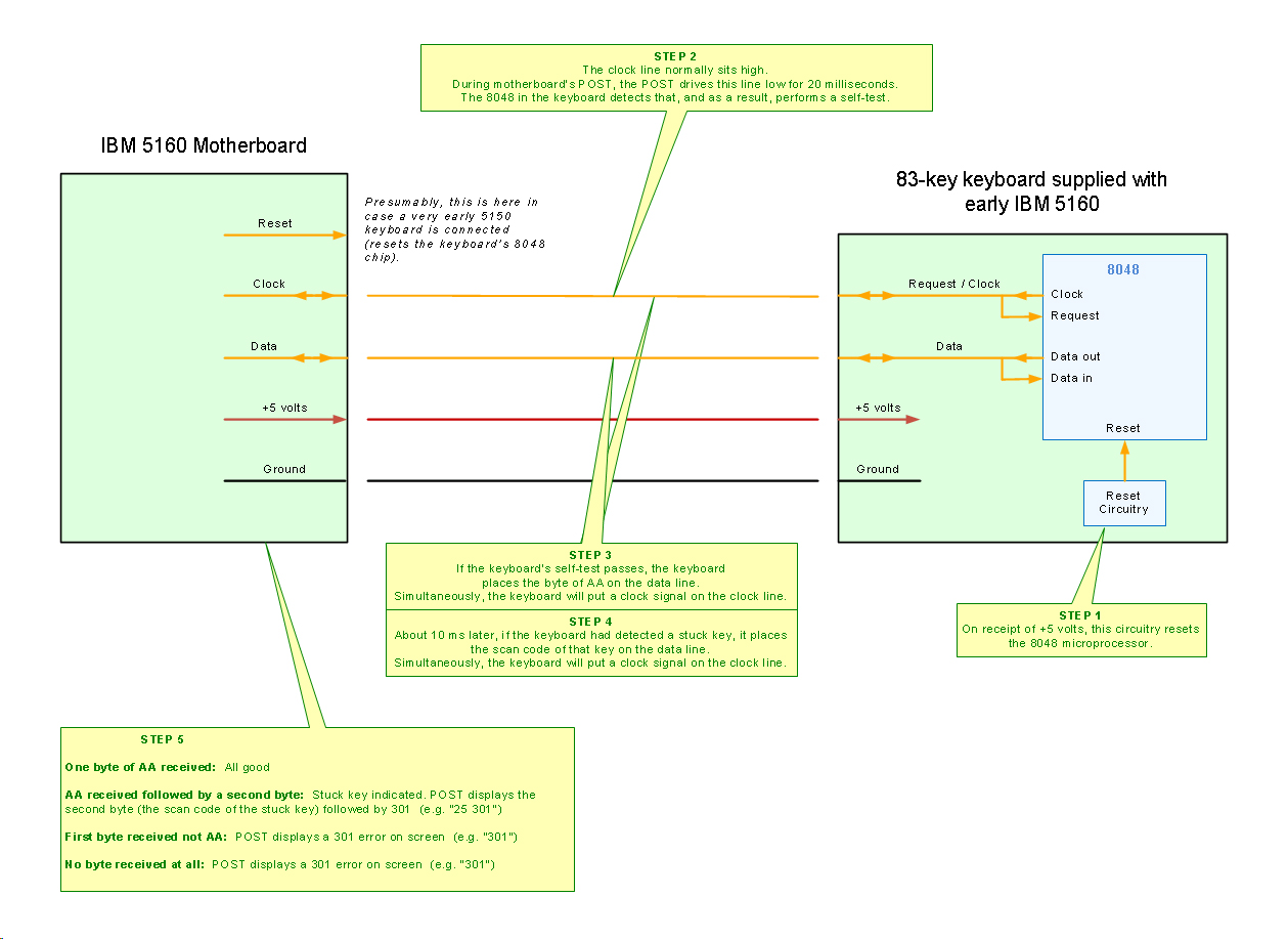
   
Note 4 The motherboard's POST uses PB6 to momentarily pull the keyboard clock line to LOW, to signal to the keyboard that the keyboard is to do a self-test.
In response, the keyboard does a self-test and then sends an AA byte to the 5160 motherboard.
See here.

(The keyboard also has the ability to pull the keyboard clock line to LOW.)
   
Note 5 Some clone XT motherboards use this bit for turbo/non-turbo control.