Home 
under_construction.gif

IBM 5162  -  The 'ground I/O CH RDY' Procedure


NOTE:  

The procedure on this web page was written specifically for the IBM 5162 motherboard.

IMPORTANT:  
JUN 2023 - Onging investigation. As it is presently written, this procedure may be fine for
some 5162 motherboards, but not others.


When to run

When ALL of the following are true:

•  Motherboard proven as faulty; and
•  Motherboard is not faulty in a way that overloads the power supply; and
•  If the motherboard has an optional 80287 NPU (or compatible) fitted, you removed it (i.e. eliminating it as the problem cause); and
•  No on-screen video; and
•  No POST beeps from the IBM BIOS ROM; and
•  You tried re-seating all socketed chips (i.e. including the 80286 CPU); and
•  A thorough visual examination of the motherboard did not reveal a problem; and
•  No error beeps from the SuperSoft diagnostic ROM; and
•  Use of an oscilloscope does not reveal pulses as expected (frequency, duration, and polarity) on pin 13 of the 8254 chip - see here.    <---- Pulses as expected indicate that the IBM BIOS ROM has started executing and has progressed at least partially.
•  
•  You have verified that the 82284A chip is generating a 16 MHz clock signal (on its pin 10), and you can observe that clock being received on the 80286 CPU (PGA pin 31), and observe it also being received on the 82288 bus controller chip (pin 2).
•  You have verified that the reset pin of the 80286 CPU is LOW.  (I.e. Verifying that CPU is not being held in a reset state.)

When all of the above are true, then a question becomes, is the 80286 CPU even able to successfully read the first word (5BEA hex) of the reset vector within the IBM BIOS ROM's.
That is what this procedure tries to establish.


More information - technical

The startup sequence of the IBM 5162 motherboard is at here.

In those pointed-to sequences, take a look at steps 8 and 9.  Those two steps can be observed using a logic analyser, but what if one does not have a logic analyser?  Well, if you have a logic probe, then by following the procedure below, you can observe part of it:
- The 80286 CPU putting address FFFFF0 (hex) onto the motherboard's address bus.
- The relevant part of address FFFFF0 going from the address bus to the address pins of the IBM BIOS ROM's (via the external address bus).
- Both IBM BIOS ROM chips being enabled (i.e. instructed to output the data they have at the presented address).
- IBM BIOS ROM chip U34 outputting the data of EA hex to the low byte of the external data bus (diagram).
- IBM BIOS ROM chip U35 outputting the data of 5B hex to the high byte of the external data bus (diagram).
- The data of 5BEA hex going from the external data bus to the data bus.
- The data of 5BEA hex going from the data bus to the data pins of the 80286 CPU.

In the procedure below, some additional steps (10 through 13) have been added to verify that there are no 'stuck bits' nor 'shorted bits' in the data direction of: IBM BIOS ROM's ---> 80286 CPU.  For those steps, you will need an EPROM programmer and some suitable EPROM's.


Not tested

A hell of a lot !!!!

Some examples:
•  No I/O operations
•  No memory write operations
•  The entire contents of the IBM BIOS ROM's - maybe some content is corrupt.
•  Data path in the direction of: 80286 CPU ---> external data bus
•  If steps 10 through 13 were not done, then data path in the direction of: external data bus ---> 80286 CPU (because maybe, in that direction, there is bit stuck HIGH or LOW, or maybe shorted bits)
•  ...
•  ...
•  ...

This procedure is a kind of, 'Well, are we at least getting to first base ?'   The result dictates the diagnostic steps that would then be done.


Test equipment required

Below, you will be measuring HIGH's and LOW's of TTL logic.  For this procedure, the best tool to use for that is a logic probe.  An oscilloscope is also suitable.

A multimeter is not suitable.  Why?  This procedure puts the motherboard into a static state (although clocks will still be present).  If some problem results in the motherboard not going into a static state, a multimeter will not reveal that, whereas a logic probe will (the probe's pulse LED will flash).

For step 10 and onward, you will need an EPROM programmer, and 27C256 type EPROM's (or equivalent).


under_construction.gif


Procedure - Step 1 of 13 - IBM BIOS ROM's

Verify that IBM BIOS ROM's are fitted.  Why?  Because we know that in the IBM BIOS ROM's, the data of 5BEA hex is expected from the ROM's when the 80286 CPU outputs address FFFFF0.  You will be looking for that 5BEA in a later step.

Step 1.1 Verify that IBM BIOS ROM's are fitted.

For the IBM 5162, these are shown at here.
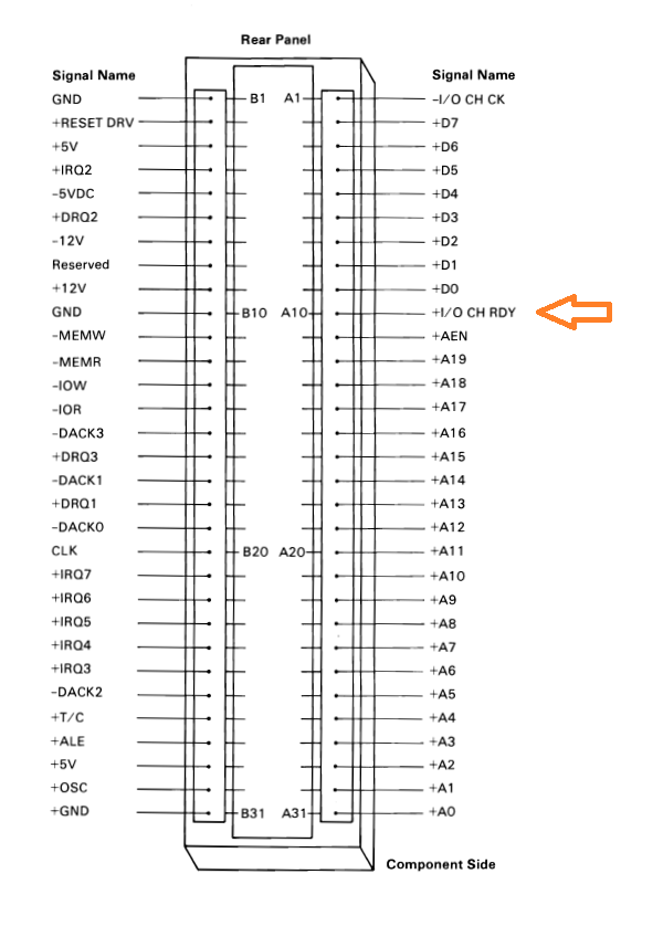
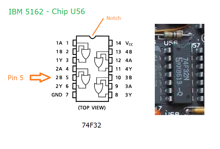
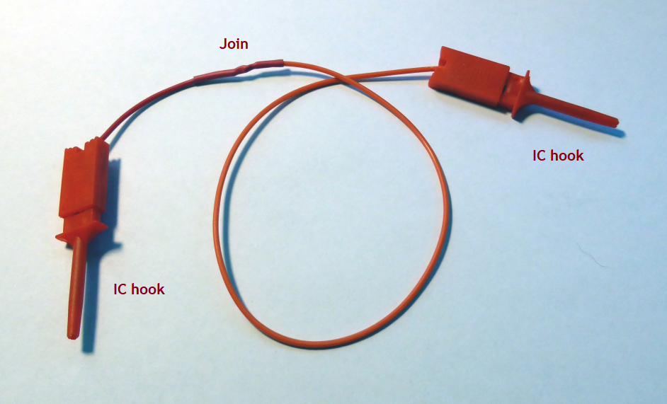
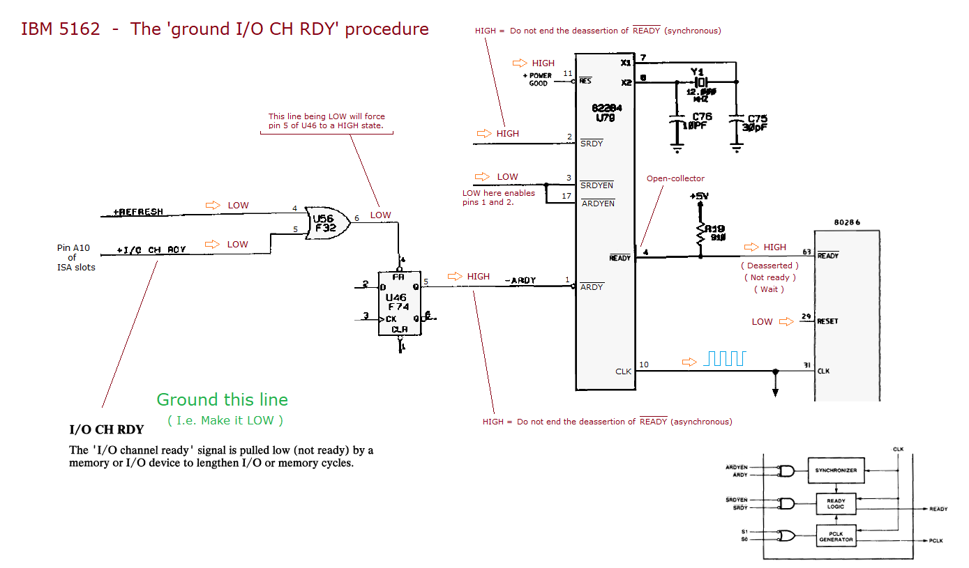

Procedure - Step 2 of 13 - Ground 'I/O CH RDY'

The goal here is that, for the duration of this procedure (all steps), the 80286 CPU's /READY pin be held HIGH at power-on time.  To do that, we could connect that pin directly to +5V, but that would carry some risk of damage to the chip that drives the 80286's /READY pin.  So instead, we are going to ground the motherboard's 'I/O CH RDY' (IOCHRDY) line.  That will result in the 80286's /READY pin being held HIGH.  A diagram is at here.

Following are some places on the 5162's motherboard where you can ground I/O CH RDY:
1.  Pin A10 of an ISA slot - see here.
2.  Pin 5 of chip U56 - see here.

Step 2.1 With power off, ground the I/O CH RDY line.

How you do the grounding is up to you, as long as it is reliable.  What I use is shown at here.

This grounding needs to remain in place for all of the following steps.
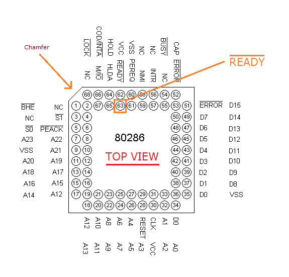
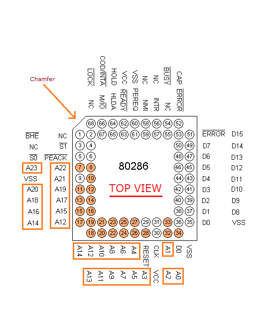


Procedure - Step 3 of 13 - Verify 80286's /READY pin is HIGH

If you have grounded I/O CH RDY correctly/properly, then we expect the /READY pin of the 80286 CPU to be HIGH.

Step 3.1 Power on the motherboard, then verify that PGA pin 63 (the /READY pin) of the 80286 CPU is HIGH - see here.

If not HIGH, use the diagram at here to see if you can work out why it is not HIGH.

Note: On pin 63, if your logic probe is showing activity (the pulse LED is flashing) or your oscilloscope is showing activity, then something is wrong.
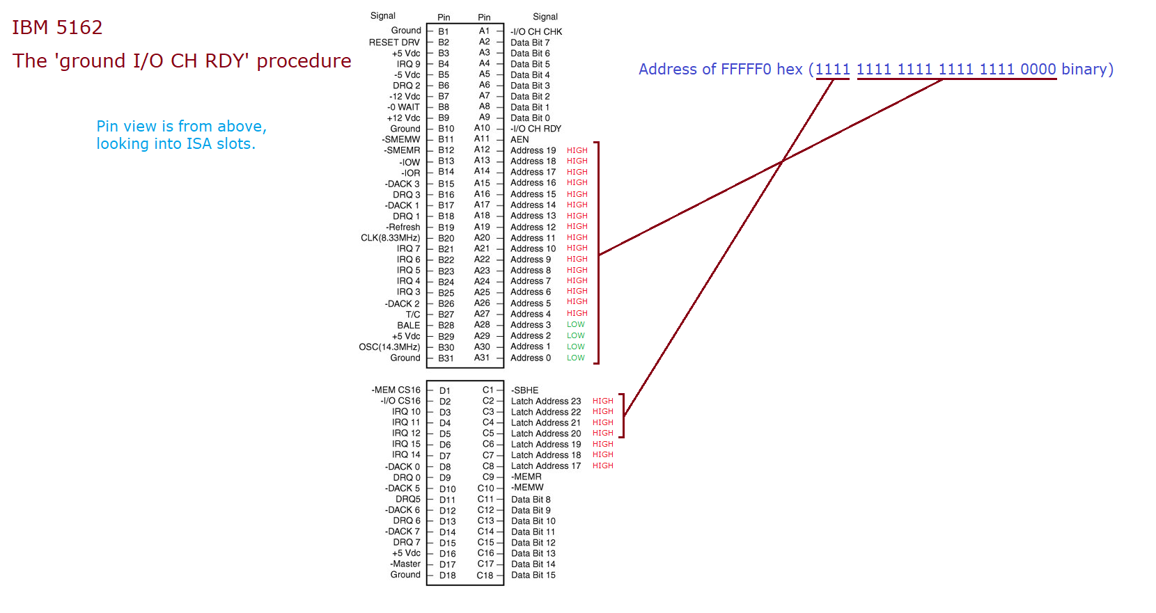


Procedure - Step 4 of 13 - Do we observe the expected address on the ISA slots?

There is no point in doing this step if the previous step did not show the expected result.

We will skip looking for address FFFFF0 hex on the address pins of the 80286 CPU.  Instead, we will look for FFFFF0 on the address pins of an ISA slot.  From an address perspective, the ISA slots are half way between the CPU and the two IBM BIOS ROM chips, U34 and U35.

Step 4.1 On the 24 address pins of an ISA slot, expect to measure the address of FFFFF0 hex (1111 1111 1111 1111 0000 binary).  See here.

If you do not see that, you need to go back to the source of the address, the 80286 CPU, and so you would verify that the address of FFFFF0 hex is at least coming out of the 80286 CPU.  See here.
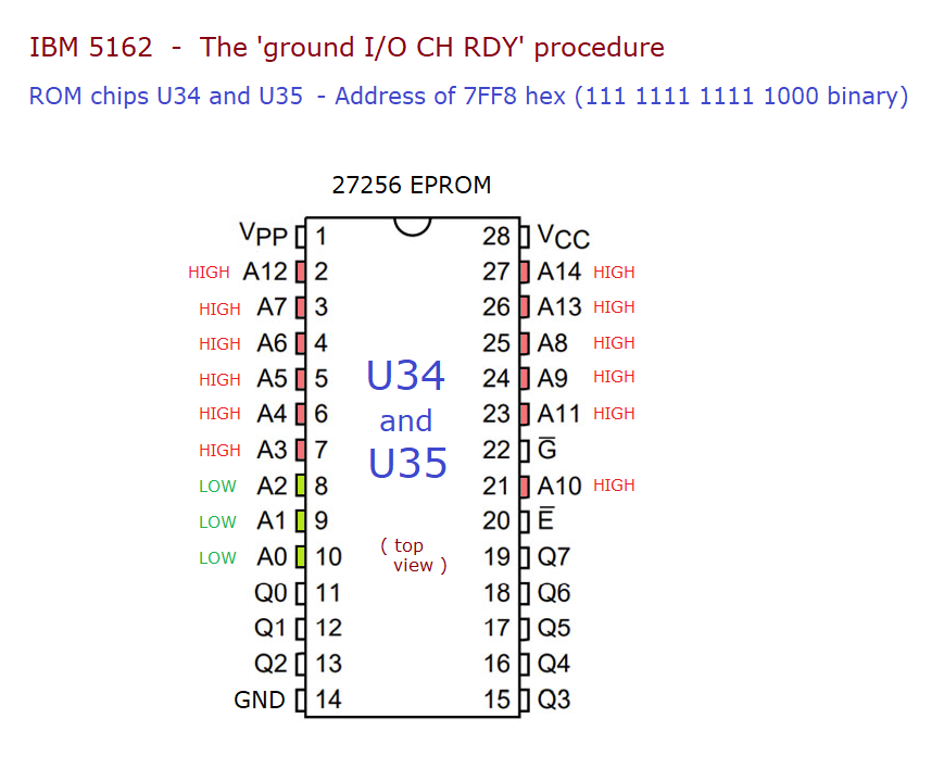


Procedure - Step 5 of 13 - Do we observe the expected address on the IBM BIOS ROM chips?

There is no point in doing this step if the previous step did not show the expected result.

Here, we are seeing if the relevant part of the FFFFF0 address is getting all the way to the two IBM BIOS ROM chips, U34 and U35.
A reference diagram is at here.

Step 5.1 On the address pins (A14 to A0) of ROM chip U34, expect to measure the address of 7FF8 hex (111 1111 1111 1000 binary).  See here.
Step 5.2 On the address pins (A14 to A0) of ROM chip U35, expect to measure the address of 7FF8 hex (111 1111 1111 1000 binary).  See here.
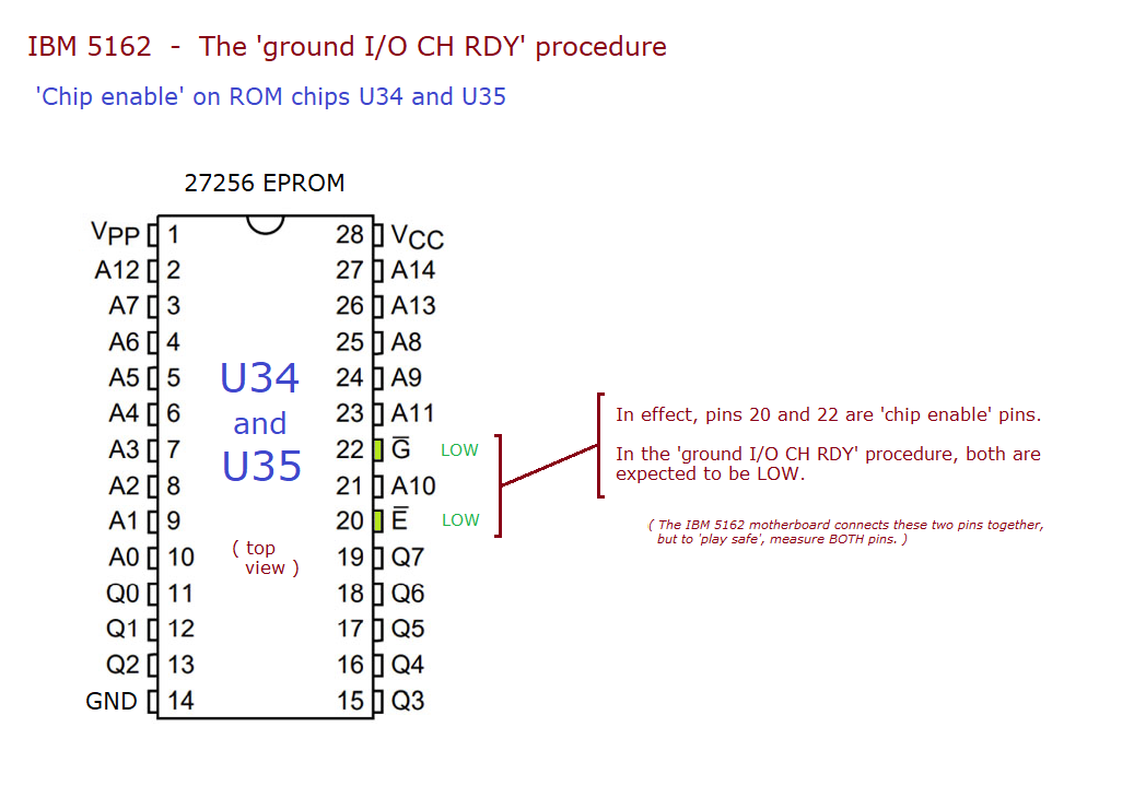
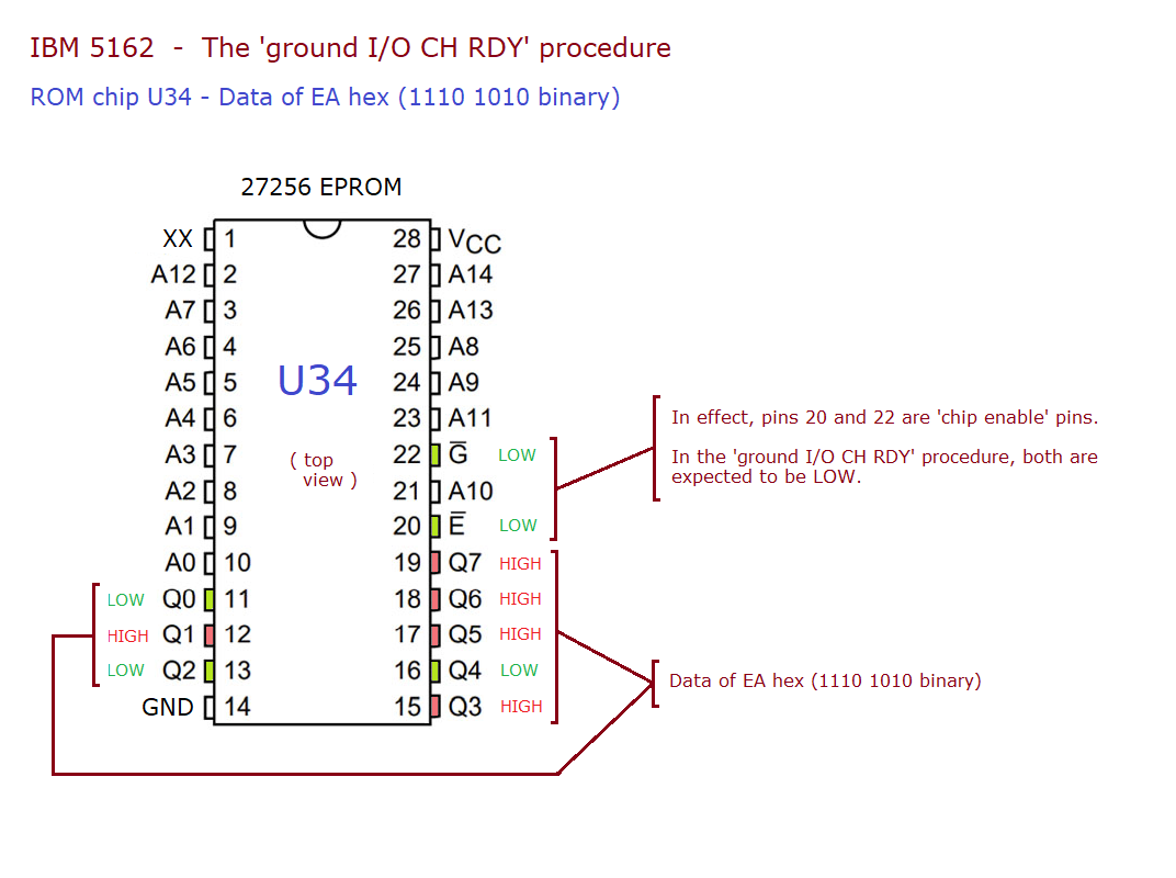
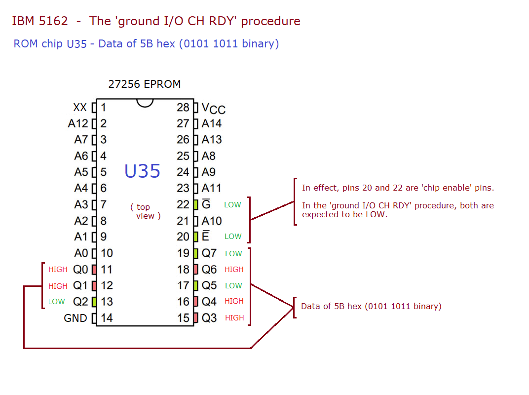


Procedure - Step 6 of 13 - Do we observe that the IBM BIOS ROM chip is enabled?

There is no point in doing this step if the previous step did not show the expected result.

At this time, certain motherboard circuitry is expected to be enabling the IBM BIOS ROM.
A reference diagram is at here.

Step 6.1 Verify that pins 20 and 22 of ROM chip U34 are LOW.  See here.
Step 6.1 Verify that pins 20 and 22 of ROM chip U35 are LOW.  See here.


Procedure - Step 7 of 13 - Do we observe the expected data out of the IBM BIOS ROM chips?

There is no point in doing this step if the previous step did not show the expected result.

We have verified that the expected address is reaching the IBM BIOS ROM chips, and that the IBM BIOS ROM chips are enabled (i.e. the ROM's will output the data they have at the presented adddress).
Therefore, we now expect to see the data of EA coming out of IBM BIOS ROM chip U34, and the data of 5B coming out of IBM BIOS ROM chip U35.

A reference diagram for the IBM 5162 is at here.

Step 7.1 On the data pins (D7 to D0) (Q7 to Q0) of ROM chip U34, expect to measure the data of EA hex (1110 1010 binary).  See here.
Step 7.2 On the data pins (D7 to D0) (Q7 to Q0) of ROM chip U35, expect to measure the data of 5B hex (0101 1011 binary).  See here.

Note: If you see the data of EA coming out of IBM BIOS ROM chip U34, and the data of 5B coming out of IBM BIOS ROM chip U35, that does not mean that those chips are 100% good.  EA and 5B are just a couple of bytes of many in those ROM's.  There could be corrupted bytes somewhere else in one (or both) of those ROM's.  Maybe a ROM has an addressing problem.  The IBM BIOS ROM chips would still be under suspicion.
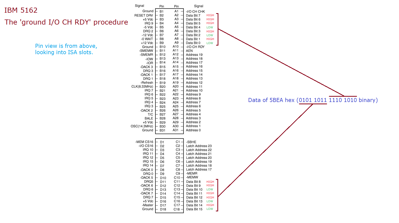


Procedure - Step 8 of 13 - Do we observe the expected data on the SD bus?

There is no point in doing this step if the previous step did not show the expected result.

Here, we are seeing if the data (5BEA) gets from the XD bus (external data bus) to the SD bus.
A convenient place to examine the SD bus is on an ISA expansion slot.
A reference diagram is at here.

Step 8.1 On the data pins of an ISA slot, expect to measure the data of 5BEA hex (0101 1011 1110 1010 binary).  See here.
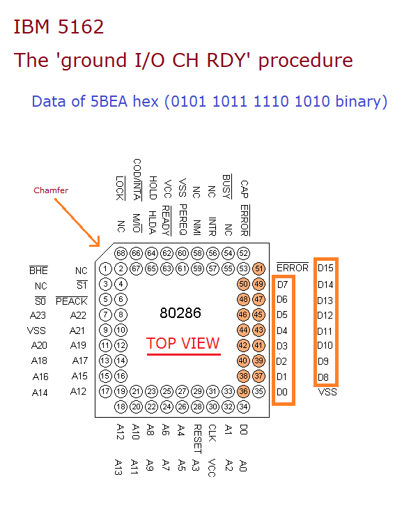


Procedure - Step 9 of 13 - Do we observe the expected data at the 80286 CPU?

There is no point in doing this step if the previous step did not show the expected result.

Here, we are seeing if the data (5BEA) gets from the SD bus to the 80286 CPU.

Step 9.1 On the data pins (D15 to D0) of the 80286 CPU, expect to measure the data of 5BEA hex (0101 1011 1110 1010 binary).  See here.


Procedure - Step 10 of 13 - ADVANCED - Exercising the data buses - All zeroes

There is no point in doing this step if the previous step did not show the expected result.

The byte of 5BEA does not 'exercise' the data buses.  This step will verify that a bit (or bits) on those buses is not stuck HIGH in the data direction of ROM --> CPU.

Exclusion: Data direction of CPU --> other things
Exclusion: The IBM BIOS ROM's - maybe a bit stuck HIGH in one of those, a bit that does not impact on the data of 5BEA hex.
Exclusion: Addressing - this is data only.

Step 10.1 Power off.
Step 10.2 Replace the two IBM BIOS ROM's with two 27C256 type EPROM's that contain 00 hex at every address.  (Replace both ROM's)
Step 10.3 Power on.
Step 10.4 On the 16 data pins (D15 to D0) of the 80286 CPU, expect to measure the data of 0000 hex (0000000000000000 binary).

Note: Taking the shortcut of measuring this on the ISA slot is only doing half the job.  The problem could be between the ISA slot and the CPU.


Procedure - Step 11 of 13 - ADVANCED - Exercising the data buses - All ones

There is no point in doing this step if the previous step did not show the expected result.

The byte of 5BEA does not 'exercise' the data buses.  This step will verify that a bit (or bits) on those buses is not stuck LOW in the data direction of ROM --> CPU.

Exclusion: Data direction of CPU --> other things
Exclusion: The IBM BIOS ROM's - maybe a bit stuck LOW in one of those, a bit that does not impact on the data of 5BEA hex.
Exclusion: Addressing - this is data only.

Step 11.1 Power off.
Step 11.2 Replace the two IBM BIOS ROM's with two 27C256 type EPROM's that contain FF hex at every address.  (Replace both ROM's)
Step 11.3 Power on.
Step 11.4 On the 16 data pins (D15 to D0) of the 80286 CPU, expect to measure the data of FFFF hex (1111111111111111 binary).

Note: Taking the shortcut of measuring this on the ISA slot is only doing half the job.  The problem could be between the ISA slot and the CPU.


Procedure - Step 12 of 13 - ADVANCED - Exercising the data buses - Shorted bits - Part 1 of 2

There is no point in doing this step if the previous step did not show the expected result.

The byte of 5BEA does not 'exercise' the data buses.  This step is one of two (steps 12 and 13) that will verify that adjacent bits on those buses are not shorted, in the data direction of ROM --> CPU.

Exclusion: Data direction of CPU --> other things
Exclusion: The IBM BIOS ROM's - maybe there are bits shorted in one of those.
Exclusion: Addressing - this is data only.

Step 12.1 Power off.
Step 12.2 Replace the two IBM BIOS ROM's with two 27C256 type EPROM's that contain 55 hex at every address.  (Replace both ROM's)
Step 12.3 Power on.
Step 12.4 On the 16 data pins (D15 to D0) of the 80286 CPU, expect to measure the data of 5555 hex (0101010101010101 binary).

Note: Taking the shortcut of measuring this on the ISA slot is only doing half the job.  The problem could be between the ISA slot and the CPU.


Procedure - Step 13 of 13 - ADVANCED - Exercising the data buses - Shorted bits - Part 2 of 2

There is no point in doing this step if the previous step did not show the expected result.

The byte of 5BEA does not 'exercise' the data buses.  This step is one of two (steps 12 and 13) that will verify that adjacent bits on those buses are not shorted, in the data direction of ROM --> CPU.

Exclusion: Data direction of CPU --> other things
Exclusion: The IBM BIOS ROM's - maybe there are bits shorted in one of those.
Exclusion: Addressing - this is data only.

Step 13.1 Power off.
Step 13.2 Replace the two IBM BIOS ROM's with two 27C256 type EPROM's that contain AA hex at every address.  (Replace both ROM's)
Step 13.3 Power on.
Step 13.4 On the 16 data pins (D15 to D0) of the 80286 CPU, expect to measure the data of AAAA hex (1010101010101010 binary).

Note: Taking the shortcut of measuring this on the ISA slot is only doing half the job.  The problem could be between the ISA slot and the CPU.


END OF PROCEDURE