| Home |
IMPORTANT: |
This procedure assumes that the 131 error is 'permanent', not intermittent. |
| 1. | For the early steps, you require a multimeter, and the knowledge of how to use it to: • Make measurements of DC voltage; and • Make measurements of resistance. |
| 2. | For the later steps (if you get that far), you require an oscilloscope, and the knowledge of how to use it to: • Make measurements of waveforms. |
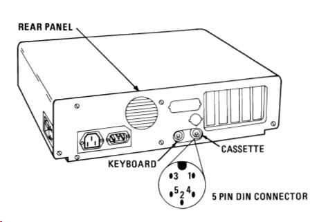
| Step 1.1 | If there is anything plugged into the DIN connector of the cassette interface, detatch it, then see if the 131 error still occurs. If the 131 disappears, then obviously, there is a problem with whatever was attatched. |
| Step 2.1 | If there are any ISA cards besides the video card, remove them, then see if the 131 error still occurs. If the 131 disappears, then obviously, one of the removed ISA cards is somehow causing the 131 error. |
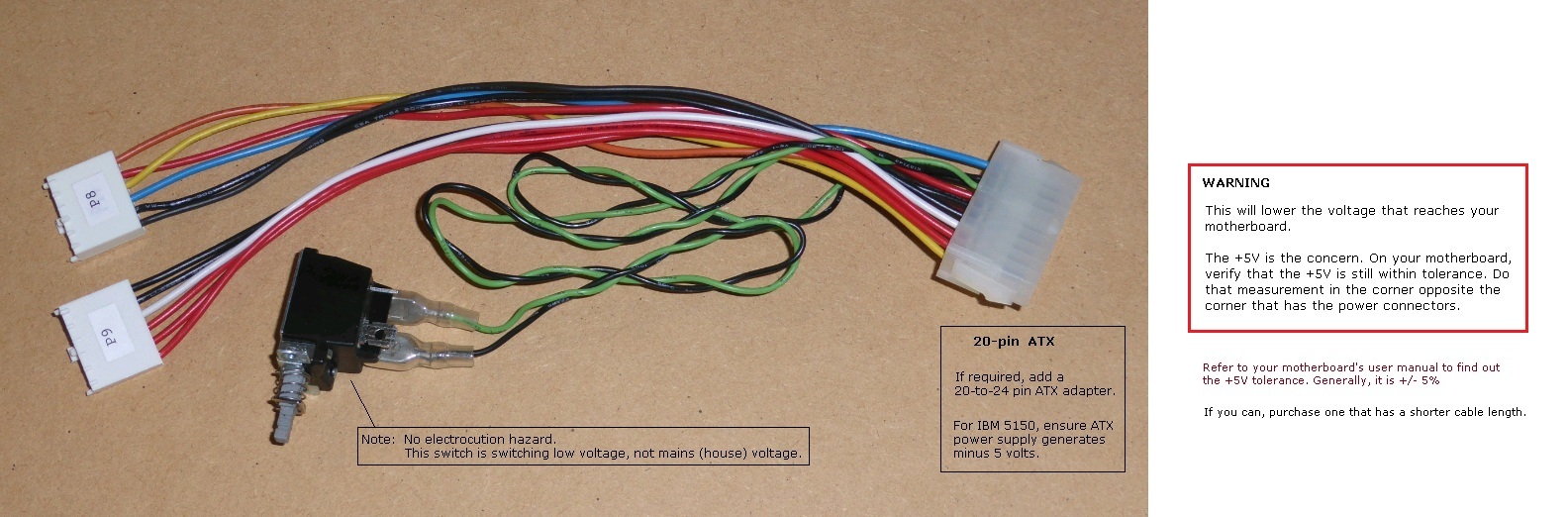
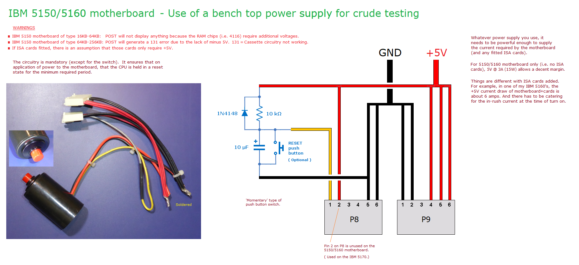
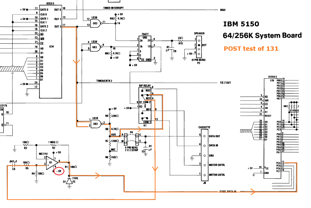
| Step 3.1 | With power on, measure the DC voltage on pin 4 of chip U1, a 741 op-amp. See here. If you measure about minus 5 volts (-5V) there, proceed on to step 4. If you don't, consider the following possibilities: • If no voltage measured, one possibility is that the probe did not piece the oxide layer on the pin. • Try reseating plug P9 from the power supply, in case of a bad connection there. • Perhaps you have a 64KB-256KB version of the 5150 motherboard, and in use is an ATX power supply (via adapter) that does not have a minus 5 volts output. • Perhaps you have a 64KB-256KB version of the 5150 motherboard, and in use is this. |
| Note: | We are measuring at the U1 chip, and not at the P9 plug from the power supply. Why? Because measuring at P9 is only 'half the job'. It does not inform us that the minus 5V is reaching all the way to chip U1. |
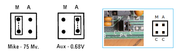
| Step 4.1 | With no power to the motherboard, remove the P4 jumper. |
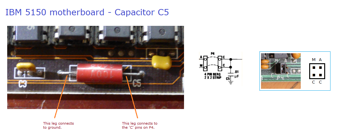
| Step 4.2 | Power on the motherboard. If the 131 error is still present, restore the P4 jumper, then proceed on to step 5. If instead, the 131 error no longer appears, consider the following possibilities: • Capacitor C5 may be short-circuit. See note 2 below for more information about this. • There may be a problem in the PCB (assumption: nothing connected to the DIN connector of the cassette interface. |
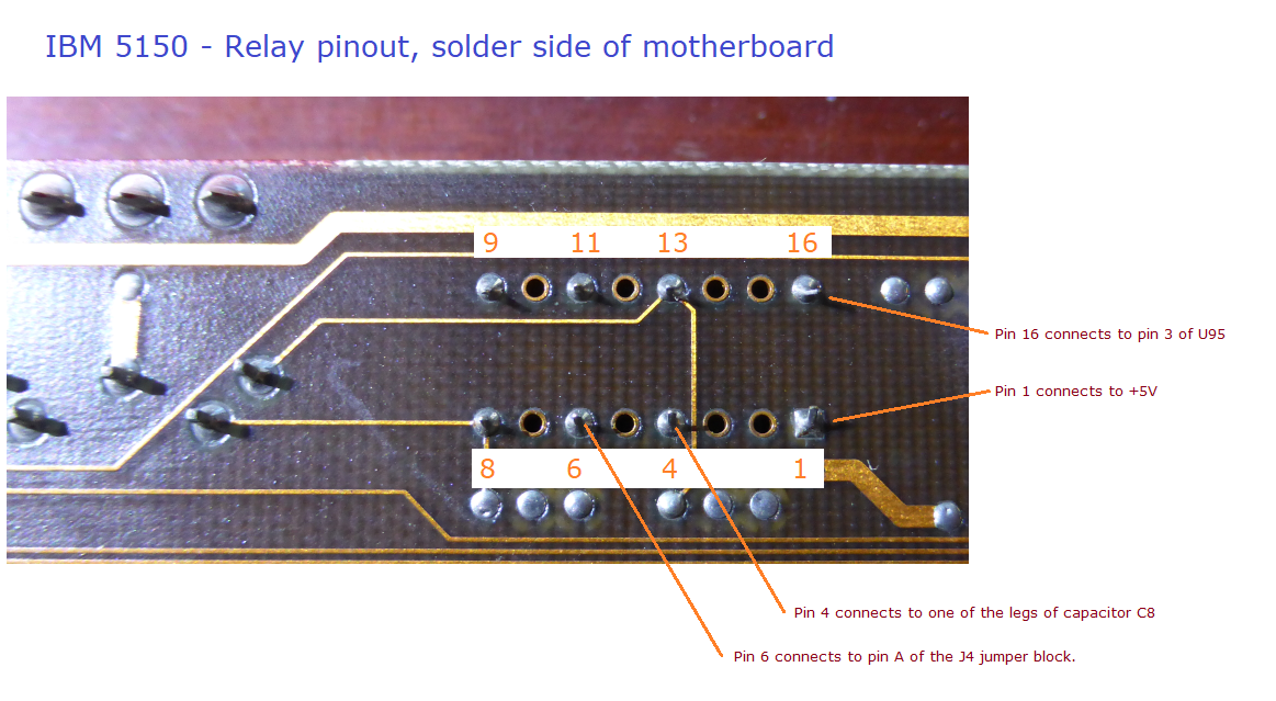
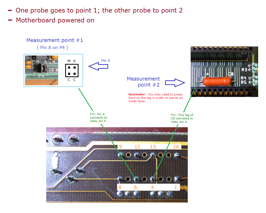
| Step 5.1 | Later, in step 5.3, you are going to measure the resistance between pins 4 and 6 of the relay. That can be done in either of two ways: • Method #1: On the solder side of the motherboard, probing pins 4 and 6 of the relay. • Method #2: On the component side of the motherboard, probing two particular points. Most people will choose method #2. With that method, the motherboard does not need to be removed from the computer. Decide which of the two you are going to do, then proceed. |
| Step 5.2 | Power ON the motherboard. <---- ON, not OFF |
| Step 5.3 | If you chose method #1, refer to the pinout diagram of the relay at here, then measure the resistance between pins 4 and 6. You may need to press the probes hard into the solder joints. (Reminder: Motherboard powered on.) If instead, you chose method #2, refer to the diagram at here, then measure the resistance between the two points. (Reminder: Motherboard powered on.) For either method, expected is a resistance between zero and, say, 20 ohms. As examples, on one good motherboard of mine, the measurement is about 4 ohms. On another good motherboard of mine, it is about 10 ohms. If you measure that, good, proceed on to step 6. If instead, there is high to infinate resistance, click here to determine what is causing that problem. |
| Note: | Some people may say that measuring the resistance between pins 1 and 3 in the cassette DIN connector will inform one as to whether the relay is off or on, and from that, infer the open/closed state of pins 4 and 6 of the relay. That is true ONLY if the relay is fully functional, and we don't know that. The 131 test needs pins 4 and 6 of the relay to be in a closed state when the motherboard is powered on, and so that is what we are measuring. |
| Step 7.1 | Power on the motherboard. |
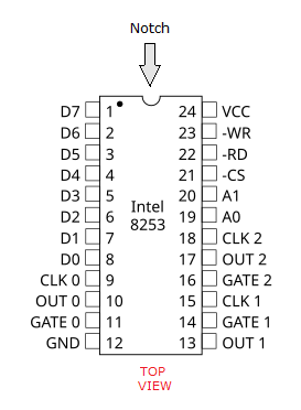
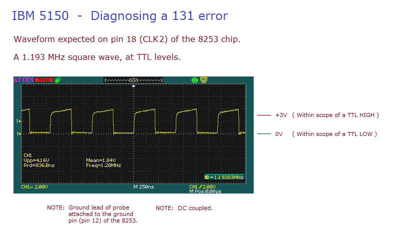
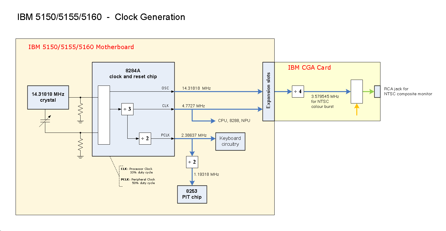
| Step 7.2 | The 8253 chip needs a 1.193 MHz clock coming into it on the CLK2 pin. Using your oscilloscope, measure the CLK2 pin (pin 18) of the 8253 chip. Pin layout diagram at here. The expected measurement is what is shown at here. If you see that, proceed to step 7.3 If you don't see that, there is a problem, and so consider the following possibilities: • You measured the wrong pin. • If no signal seen, one possibility is that the probe did not piece the oxide layer on the pin. • You operated your oscilloscope incorrectly. • Certain other circuitry is not generating the 1.193 MHz clock. • The 8253 is faulty in a particular way, impacting on its CLK0 or CLK1 or CLK2 pin. |
| Step 7.3 | Before proceeding, ensure that the 131 error has appeared. <---- IMPORTANT (see note 1) |
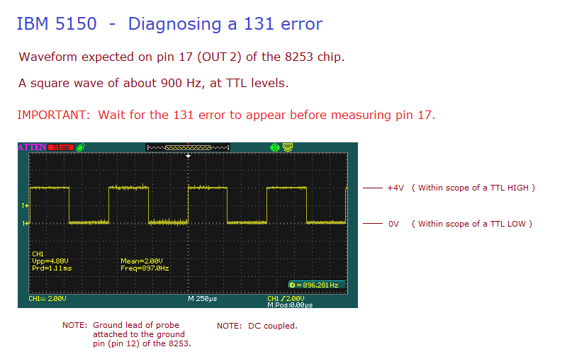
| Step 7.4 | Using your oscilloscope, measure the OUT2 pin (pin 17) of the 8253 chip. Pin layout diagram at here. The expected measurement is what is shown at here, a square wave of about 900 Hz at TTL levels. If you see that, proceed to step 8. If you don't see that, there is a problem, and so consider the following possibilities: • You measured the wrong pin. • If no signal seen, one possibility is that the probe did not piece the oxide layer on the pin. • You operated your oscilloscope incorrectly. • Faulty 8253 chip. • There may be a problem in the PCB. • Chip U63 is faulty in a particular way, that impacts on the OUT2 pin of the 8253 chip. |
| Step 8.1 | Power on the motherboard. |
| Step 8.2 | Wait for the 131 error to appear. <---- IMPORTANT (see note 1) |
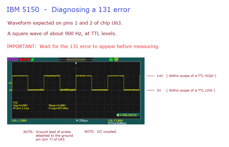
| Step 8.3 | Using your oscilloscope, measure pin 1 of chip U63. Pin layout diagram at here. The expected measurement is what is shown at here, a square wave of about 900 Hz at TTL levels. If you see that, proceed to step 8.4 If you don't see that, there is a problem, and so consider the following possibilities: • You measured the wrong pin. • If no signal seen, one possibility is that the probe did not piece the oxide layer on the pin. • You operated your oscilloscope incorrectly. • There may be a problem in the PCB, between the 8253 chip and chip U63. |
| Step 8.4 | Pins 1 and 2 of chip U63 are connected together by the PCB. Although we checked pin 1 in the previous step, we should verify pin 2 as well. Using your oscilloscope, measure pin 2 of chip U63. Pin layout diagram at here. The expected measurement is what is shown at here, a square wave of about 900 Hz at TTL levels. If you see that, proceed to step 8.5 If you don't see that, there is a problem, and so consider the following possibilities: • You measured the wrong pin. • If no signal seen, one possibility is that the probe did not piece the oxide layer on the pin. • You operated your oscilloscope incorrectly. • There may be a problem in the PCB, between pins 1 and 2 on chip U63. |
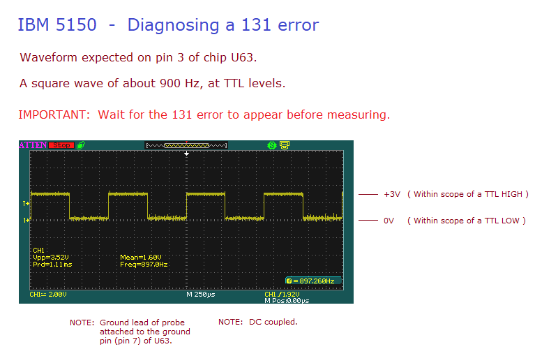
| Step 8.5 | Using your oscilloscope, measure pin 3 of chip U63. Pin layout diagram at here. The expected measurement is what is shown at here, a square wave of about 900 Hz at TTL levels. If you see that, proceed to step 9. If you don't see that, there is a problem, and so consider the following possibilities: • You measured the wrong pin. • If no signal seen, one possibility is that the probe did not piece the oxide layer on the pin. • You operated your oscilloscope incorrectly. • Faulty chip U63. |
| Step 9.1 | Power on the motherboard. |
| Step 9.2 | Wait for the 131 error to appear. <---- IMPORTANT (see note 1) |
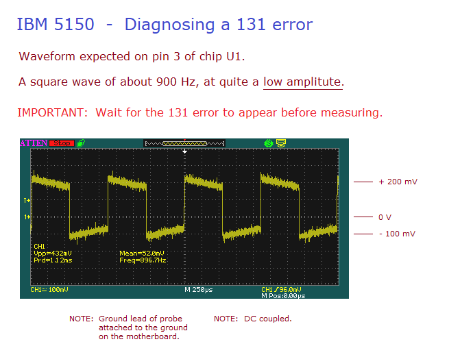
| Step 9.3 | Using your oscilloscope, measure pin 3 of chip U1, a 741 op-amp. Pin layout diagram at here. The expected measurement is what is shown at here. If you see that, proceed to step 9.4 If you don't see that, there is a problem, and so consider the following possibilities: • You measured the wrong pin. • If no signal seen, one possibility is that the probe did not piece the oxide layer on the pin. • You operated your oscilloscope incorrectly. • There may be a problem in the PCB, between chip U63 and chip U1. |
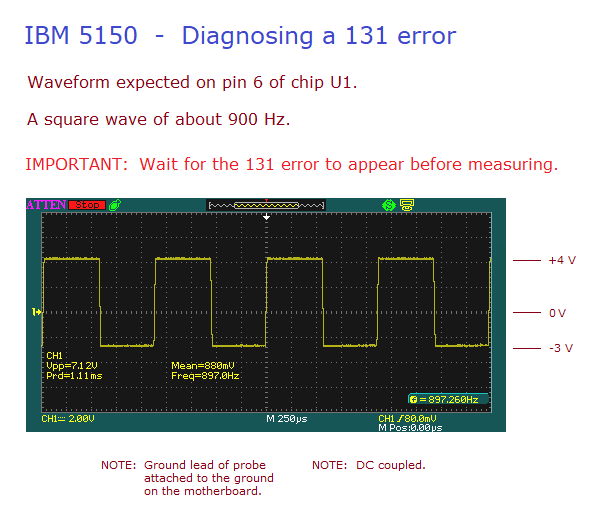
| Step 9.4 | Using your oscilloscope, measure pin 6 of chip U1, a 741 op-amp. Pin layout diagram at here. The expected measurement is what is shown at here. If you see that, proceed to step 10 If you don't see that, there is a problem, and so consider the following possibilities: • You measured the wrong pin. • If no signal seen, one possibility is that the probe did not piece the oxide layer on the pin. • You operated your oscilloscope incorrectly. • Faulty U1 chip. • There may be a problem in the PCB. |
| Step 10.1 | Power on the motherboard. |
| Step 10.2 | Wait for the 131 error to appear. <---- IMPORTANT (see note 1) |
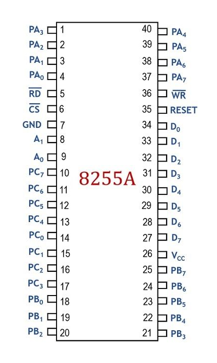
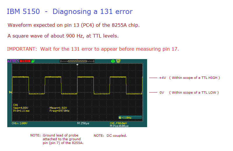
| Step 10.3 | Using your oscilloscope, measure pin 13 (PC4) of the 8255A chip (U36). Pin layout diagram at here. The expected measurement is what is shown at here, a square wave of about 900 Hz at TTL levels. If you see that, it is most likely that the 8255A chip is partially faulty (in a way that affects it's PC4 input). If you don't see that, there is a problem, and so consider the following possibilities: • You measured the wrong pin. • If no signal seen, one possibility is that the probe did not piece the oxide layer on the pin. • You operated your oscilloscope incorrectly. • There may be a problem in the PCB, between the chip U1 and the 8255A chip. |
| Note 1 | There is a delay before the POST programs/configures the 8253 chip to generate the tone for the 131 test, and turns off the relay. When you see the '131' on-screen, you know that the POST has done both. |
| Note 2 | On my IBM 5150 motherboard, I can produce a 131 error by having the P4 jumper set to the A-to-C position and shorting out capacitor C5. ( No 131 error if the P4 jumper is set to the M-to-C position. ) |